

 +91 9840476397
 VLSI Training in Chennai
Are you Looking for VLSI Training in Chennai? Want to learn real time hand on experienced trainers? Don’t worry Wiztech Automation is here, Call at +91 9940 426 826.
Wiztech Automation Solutions is the Best VLSI Training in Chennai, because of Job oriented Advanced VLSI Training with real time practical oriented approach. For freshers we offer placement oriented vlsi course with attractive scholarships.Very-large-scale integration
Very-large-scale integration (VLSI) is the process of creating an integrated circuit (IC) by combining thousands oftransistorsinto a single chip. VLSI began in the 1970s when complex semiconductor and communication technologies were being developed. The microprocessor is a VLSI device. VLSI Training in Chennai Before the introduction of VLSI technology, most ICs had a limited set of functions they could perform. Anelectronic circuitmight consist of aCPU, ROM, RAMand otherglue logic. VLSI lets IC designers add all of these into one chip. The electronics industry has achieved a phenomenal growth over the last few decades, mainly due to the rapid advances in large scale integration technologies and system design applications. With the advent of very large scale integration (VLSI) designs, the number of applications of integrated circuits (ICs) in high-performance computing, controls, telecommunications, image and video processing, and consumer electronics has been rising at a very fast pace. The current cutting-edge technologies such as high resolution and low bit-rate video and cellular communications provide the end-users a marvelous amount of applications, processing power and portability. This trend is expected to grow rapidly, with very important implications on VLSI design and systems design. VLSI Training in ChennaiVLSI Design Flow
The VLSI IC circuits design flow is shown in the figure below. The various levels of design are numbered and the blocks show processes in the design flow. Specifications comes first, they describe abstractly, the functionality, interface, and the architecture of the digital IC circuit to be designed.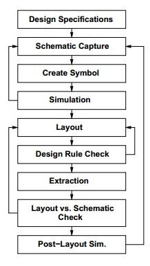
Behavioral description is then created to analyze the design in terms of functionality, performance, compliance to given standards, and other specifications. RTL description is done using HDLs. This RTL description is simulated to test functionality. From here onwards we need the help of EDA tools. RTL description is then converted to a gate-level netlist using logic synthesis tools. A gatelevel netlist is a description of the circuit in terms of gates and connections between them, which are made in such a way that they meet the timing, power and area specifications. Finally, a physical layout is made, which will be verified and then sent to fabrication.
Y Chart
The Gajski-Kuhn Y-chart is a model, which captures the considerations in designing semiconductor devices. The three domains of the Gajski-Kuhn Y-chart are on radial axes. Each of the domains can be divided into levels of abstraction, using concentric rings. At the top level (outer ring), we consider the architecture of the chip; at the lower levels (inner rings), we successively refine the design into finer detailed implementation - Creating a structural description from a behavioral one is achieved through the processes of high-level synthesis or logical synthesis. VLSI Training in Chennai Creating a physical description from a structural one is achieved through layout synthesis.

Design Hierarchy-Structural
The design hierarchy involves the principle of "Divide and Conquer." It is nothing but dividing the task into smaller tasks until it reaches to its simplest level. This process is most suitable because the last evolution of design has become so simple that its manufacturing becomes easier. We can design the given task into the design flow process's domain (Behavioral, Structural, and Geometrical). To understand this, let’s take an example of designing a 16-bit adder, as shown in the figure below.
 Here, the whole chip of 16 bit adder is divided into four modules of 4-bit adders. Further, dividing the 4-bit adder into 1-bit adder or half adder. 1 bit addition is the simplest designing process and its internal circuit is also easy to fabricate on the chip. Now, connecting all the last four adders, we can design a 4-bit adder and moving on, we can design a 16-bit adder.
VLSI Training in Chennai
Here, the whole chip of 16 bit adder is divided into four modules of 4-bit adders. Further, dividing the 4-bit adder into 1-bit adder or half adder. 1 bit addition is the simplest designing process and its internal circuit is also easy to fabricate on the chip. Now, connecting all the last four adders, we can design a 4-bit adder and moving on, we can design a 16-bit adder.
VLSI Training in Chennai
